Rapid prototype production of electronic assemblies
Printed Circuit Boards

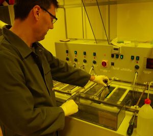
In our in-house PCB laboratory, we produce multilayer PCBs in professional quality for our development team as well as in smaller quantities on customer request.
=> A circuit modification including a change of the PCB layout and production of a new PCB version is only a matter of a few hours for our engineers.
Gerade diese Schnelligkeit verschafft uns und unseren Kunden einen wichtigen Wettbewerbsvorteil.
It is precisely this rapid production that gives us and our customers a key competitive advantage.
Available PCB substrates include both FR4 and HF materials (e.g.: Panasonic, Rogers). We can also manufacture flexible PCBs on demand.
Mechanical work

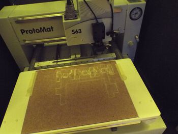
Our prototype laboratory is also equipped with CNC milling and drilling machines, which allow us to carry out mechanical work at short notice.
In addition to PCBs, plastic parts and thin metal sheets can also be milled.
Furthermore, it is possible to produce samples of parts by fine etching of copper sheets, which will later be produced as stamped-bent parts.
Manual PCB assembly

In our prototype production process, PCBs can be assembled manually or, for larger quantities or even small series, with the help of automatic assembly machines.
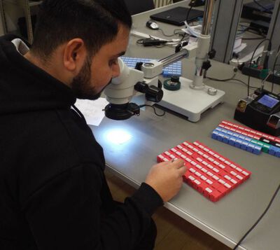
For small quantities and with a small number of components to be assembled, manual assembly is the best option due to time and cost reasons. The components are placed under the microscope and connected to the board by hand soldering.
Soldering stations from JBC and Weller in different capacities and soldering tips of various sizes ensure that soldering of components and PCBs in variable sizes and shapes are possible and handled with care.
Alternatively, if the thermal mass of the components is large, solder paste is applied, the components are placed and the solder is melted either in a reflow oven or in the vapour phase soldering system. Especially in vapour phase soldering machine, a continuous and uniform heating of the complete assembly is achieved without exceeding the permissible temperature of the components.
For soldering tin, we use Almit rolls of high-quality, lead-free solder wire of various diameters and melting temperatures as well as solder pastes of various grain sizes.
Resistors, capacitors and coils in the most common SMD types 0201, 0402 and 0603 with narrow tolerances are available as standard components. If special components (ICs and passive) are required, we will be pleased to take over the procurement of the components for you.
For the efficient assembly of small series, we utilize stencil printers, automatic assembly machines and a large vapour phase soldering machine.
Chipbonding

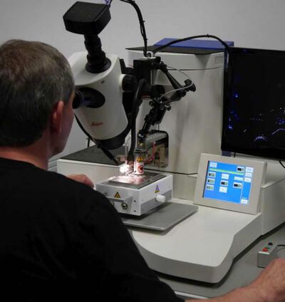
For the asssembly of unpackaged ICs onto the PCB we utilize a semi-automatic die bonder and a semi-automatic wire bonder in house.
For wedge-wedge bonding, the Wirebonder (HB16 from TPT) can be used to create a connection between the connection pads on the IC and the counterparts on the PCB. As an alternative, ball wedge bonding can also be used with gold wire. The minimum pad size on the IC for this is approx. 65µm x 65µm, whereby the centre distance between adjacent pads should be at least 120µm. The most important specifications for wire bonding in our company are:
- Ball-wedge bonding with gold wire: wire thickness 17um to 75um
- Wedge-wedge bonding with gold and aluminium wire: wire thickness 17um to 75um
- Tape bonding: max. 25um x 250um
TPT's HB75 die bonder is used for gluing the dies and, if necessary, sealing the bonded IC (glob top) after wire bonding. With this bonder, the adhesive for the IC is applied to the PCB via a suitable stamp and then the IC is placed precisely and reproducibly on the bonding area with vacuum tweezers.
For the application of the glob top after wire bonding we have access to different 2-component epoxies. The epoxy is applied with a dispenser attached to the holder of the bonding arm. The amount of epoxy supplied is reproducibly distributed by regulating the working pressure and the valve opening time on the dispenser unit.
The curing of the adhesive or glob tops takes place in a temperature-controlled oven, in which different temperature profiles for curing can be programmed.

